To-date, the ability to reliably assess the real potential of novel semiconductor candidates at early stages of their discovery using “conventional” methods is rather limited, often via computational theory. Experimental characterization only happens later, often involving constructing full device structure, introducing additional variables. Thus, for assessing the real potential for applications of novel semiconductors, early-stage experimental characterization to unravel structure-property-performance relations (and bridge the theory-experiment gap) is crucial, but is mostly missing.

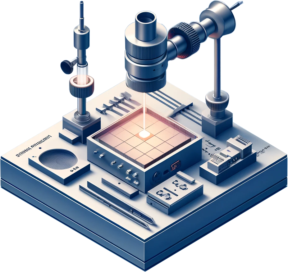
SPV spectroscopy is based on probing the charge separation of photoexcited carriers under light excitation with varying wavelengths, and allows to probe changes in the surface potential upon preferential separation of different photoexcited charge carriers.1,2 In our lab, instead of using the “conventional” vibrating Kelvin Probe (KP) technique to measure the surface potential, we use the Fixed-Capacitor probe configuration (FC-SPV, see Figure below) and use either a modulated or pulsed light excitation source. The main advantages of FC-SPV compared to “conventional” SPV based on a Kelvin Probe, relies on the fact that the probe is mechanically fixed, allowing us to use modulated light excitation combined with lock-in detection, resulting in significantly higher sensitivities (3-4 orders of magnitudes gain). Thus, by carefully performing sub-band gap SPV spectroscopy, defect-related transitions can be directly detected.
Ultraviolet photoelectron spectroscopy (UPS) is a specialized variant of photoelectron spectroscopy used to study the electronic structure of materials. In UPS, ultraviolet (UV) photons with specific energy levels are directed at a sample, causing the emission of electrons from its surface. These emitted electrons, known as photoelectrons, carry information about the sample’s electronic states and energy levels.
CFSYS has a similar working principle as the “conventional” common UPS method.3,4 The main difference between UPS and CFSYS lies in the detection mode and excitation source. In CFSYS, rather than using a single excitation wavelength and detecting the different kinetic energies of the emitted electrons, the analyzer is set to detect one specific kinetic energy (usually slightly above the Vacuum Level) and instead of the He-1 photon source (photon energy of 21.2 eV) used for UPS, for CFSYS, a near-UV source is coupled with a monochromator to excite the sample with variable photon energies between 3.7 to 7.3 eV. These differences result in a significantly higher S/N with much larger dynamic range compared to UPS, gaining several orders of magnitudes (as shown in the Figure below), thus allowing for the detection of low deep defect densities down to 1015 cm-3.
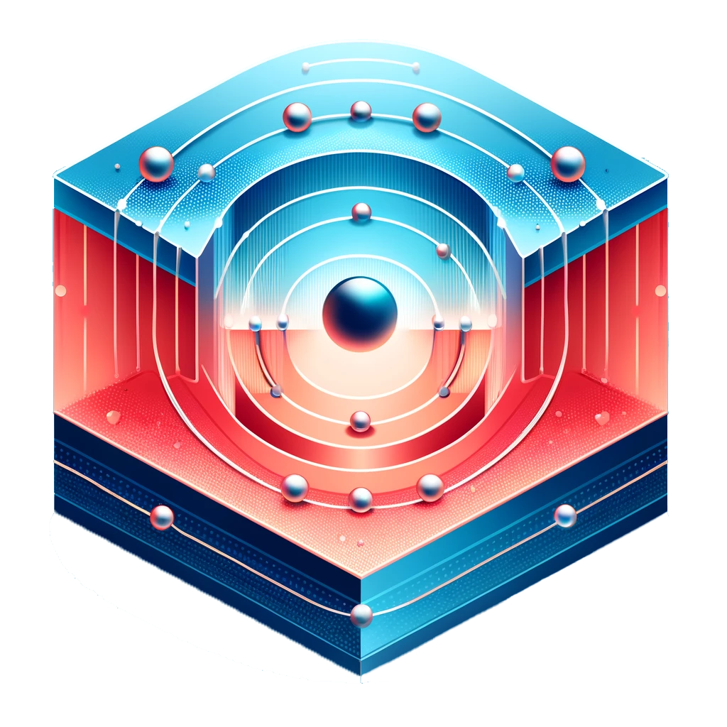
Interfaces play a pivotal role in optoelectronic devices, serving as the crucial junctions where photons and electrons meet and interact. These interfaces are the linchpin in devices such as photodetectors, solar cells, and light-emitting diodes (LEDs). In photodetectors, interfaces are responsible for efficiently converting incoming photons into electrical signals, enabling the detection of light with high sensitivity. Solar cells heavily rely on interfaces to capture and convert sunlight into electricity, and their efficiency is directly linked to the quality of these interfaces. Additionally, in LEDs, interfaces are essential for facilitating the injection and recombination of charge carriers, enabling the emission of light. Therefore, optimizing interfaces in optoelectronic devices is paramount to enhancing their performance, energy efficiency, and applicability in various fields, including telecommunications, renewable energy, and display technologies.

In our lab we use time-resolved SPV (tr-SPV) as the main tool in investigate the photogenerated charge carrier dynamics across interfaces. By combining tr-SPV with time-resolved photoluminiscence (tr-PL), we determine the dominant loss mechanism, as well the charge injection rates between the different layers across the interface, paving the route to increasing the efficiencies of various optoelectronic devices.
We study a large variety of buried interfaces such as novel 3D semiconductors with 2D semiconductors/organic molecular monolayers/biological molecules and liquid electrolytes, to open routes for novel high-efficiency hybrid optoelectronic devices.
In addition, we explore innovative defect passivation strategies, in order to mitigate non-radiative recombination losses and significantly enhance the performance and efficiency of optoelectronic devices.

At The Defect Spectroscopy Research Lab, we are constantly pushing the boundaries of defect spectroscopy research to find new solutions for energy conversion applications. Our team of experts is dedicated to discovering new and stable photoactive materials that are essential for a carbon-neutral economy. In our research, we utilize cutting-edge technology and innovative techniques to overcome experimental challenges and unravel the complex relationships between material structures and their optical properties. We have already made several breakthroughs in our research and have been published in several high impact journals. Our innovations have the potential to revolutionize the field and pave the way for a brighter, more sustainable future.

Our innovations have the potential to revolutionize the field and pave the way for a brighter, more sustainable future. We have already made several breakthroughs in our research and have been published in several high impact journals.

Explore our publications and learn more about our research.

Lorem ipsum dolor sit amet, consectetur adipiscing elit. Ut elit tellus, luctus nec ullamcorper mattis, pulvinar dapibus leo.
Lorem ipsum dolor sit amet, consectetur adipiscing elit. Ut elit tellus, luctus nec ullamcorper mattis, pulvinar dapibus leo.
Lorem ipsum dolor sit amet, consectetur adipiscing elit. Ut elit tellus, luctus nec ullamcorper mattis, pulvinar dapibus leo.
Lorem ipsum dolor sit amet, consectetur adipiscing elit. Ut elit tellus, luctus nec ullamcorper mattis, pulvinar dapibus leo.