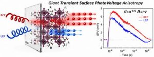
Do we always need electrical contacts to measure the CISS...

🎉 Our first paper from the Defect Spectroscopy Research Lab...
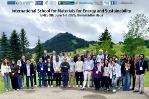
We are delighted to announce that our M.Sc. student, Israa...

We are pleased to share that our M.Sc. student, Liad...
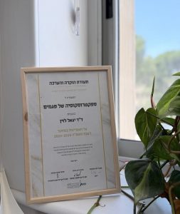
A proud moment for our lab! We are delighted to...
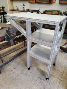
Finally after weeks of planning, we bring the last piece...

Thanks everyone for joining our group hike to Nahal Prat,...

Thanks to Idan we now have a new beautiful website...

We utilize Surface PhotoVoltage (SPV) and near-UV photoelectron Spectroscopy in order to map the energetic positions of gap states in semiconductors with extremely high sensitivity

We utilize a combination of time-resolved Surface PhotoVoltage and photoluminescence in order to probe charge transfer processes across interfaces and eliminate non-radiative losses. We then simulate and correlate our findings to actual optoelectronic device data